The Great Wall of High Bandwidth Memory (HBM)
· 28 min read
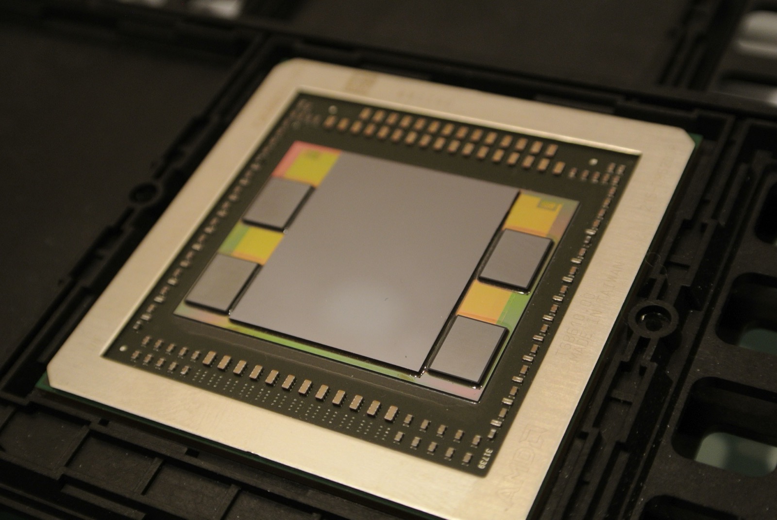 The anatomy of the AI era, in miniature: the large central die is the processor, and the four slabs hugging it are stacks of High Bandwidth Memory — all on a shared slice of silicon. This is an AMD Fiji package. Photo: C. Spille / pcgameshardware.de, CC BY-SA 4.0, via Wikimedia Commons.
On June 25, 2026, the artificial intelligence insurgence quietly arrived at the cash register of your local Apple Store.
In a move almost without precedent, Apple raised prices across nearly its entire consumer lineup. The entry-level MacBook Neo — the machine pitched at students and the budget-conscious — jumped from $599 to $699, mere months after launch. The base 11-inch iPad Air climbed $150 to $749. The 14-inch MacBook Pro went up $300. The high-end Mac Studio M3 Ultra leapt an eye-watering $1,300 to $5,299. Even aging refurbished stock and the HomePod got swept up in the repricing.
The culprit wasn't a shortage of Apple's own silicon, or a spike in the cost of milled-aluminum cases. In a rare moment of candor, Apple — and outgoing CEO Tim Cook — pointed at a single structural bottleneck: an extraordinary surge in the price of memory chips. Cook called the situation "unsustainable," a "hundred-year flood" of demand. Apple's stock fell nearly 6 percent on the news, its steepest drop since the tariff panics of the year before.
What's happening is a violent, zero-sum reshuffling of the entire global semiconductor supply chain. To feed the bottomless data appetite of AI training and inference, the world's memory makers have yanked their factories away from the ordinary memory (DRAM) inside laptops and phones, and redirected their cash and cleanroom space toward a fiendishly difficult, monstrously expensive technology called High Bandwidth Memory, or HBM.
Here's the brutal arithmetic: because HBM needs special manufacturing, longer production cycles, and far more silicon real estate, every wafer devoted to AI memory eats up the capacity that would have made roughly three wafers of standard DRAM. Industry insiders call it the "capacity penalty." The result is a hyper-inflation in ordinary memory that analysts have nicknamed "RAM-ageddon." Contract DRAM prices rose 58 to 63 percent in the second quarter of 2026 alone, with spikes of over 125 percent projected into 2027.
To understand why a giant language model inference in an Ohio data center makes an iPad more expensive in Tokyo, you have to go down — way down — into the microscopic, 55 billion dollar architecture of HBM. It's a technology defined by extreme physical constraints, controlled by a fragile three-company cartel, secretly dependent on a handful of Japanese chemical suppliers, and increasingly the single most important arbiter of who wins the global AI race.
The architecture of a bottleneck
High Bandwidth Memory isn't a new kind of memory cell. It's a radical, three-dimensional rethink of how you package memory.
For decades, memory chips have sat beside the processor on a circuit board, chatting with it over relatively narrow data highways. That worked fine — until the processors changed. As the Graphics Processing Units (GPUs) made by Nvidia and AMD got exponentially better at the massive matrix multiplication that generative AI demands, they slammed into something engineers call the "Memory Wall." The processor could crunch numbers far faster than the memory could deliver them. The chip was, in effect, starving — a Formula 1 engine fed through a drinking straw.
HBM tears down that wall by stacking, not spreading. Engineers take multiple DRAM chips, grind them down to a fraction of the width of a human hair, and stack them vertically like microscopic pancakes. That stack sits on top of a foundational "base die" and is placed just millimeters from the GPU, on a shared slab of silicon called an interposer. (The packaging technology that makes this possible is TSMC's CoWoS — "chip-on-wafer-on-substrate.") Data shoots straight up and down through thousands of microscopic copper tunnels — Through-Silicon Vias, or TSVs — that pierce every layer of the stack.
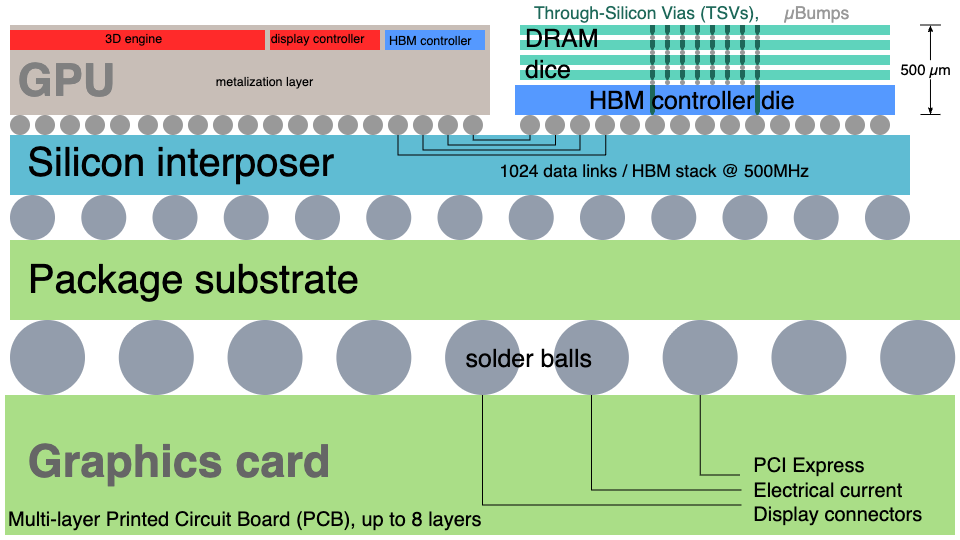 How HBM works: DRAM dies are stacked vertically on a logic base die and linked to the processor through a silicon interposer. The vertical pillars threading the stack are through-silicon vias (TSVs). Diagram: ScotXW, CC BY-SA 4.0, via Wikimedia Commons.
The payoff is a memory connection of absurd width. Where a standard memory chip might talk over a 64- or 128-bit channel, HBM3E uses a 1,024-bit interface — picture widening a 64-lane road into a thousand-lane superhighway — delivering more than 1.15 terabytes per second per stack. A modern Nvidia Blackwell B200 accelerator surrounds its logic core with eight such stacks, forming one giant pool of memory that can pour trillions of AI parameters into the compute engine almost instantly.
But physics charges a steep toll. An HBM stack runs blisteringly hot, demands atomic-level alignment, and only works if every single die in an 8- or 12-layer tower is flawless. That difficulty has consolidated the market into a tense triopoly — and the entire AI boom now leans on just three companies.
| HBM supplier | Est. market share (2025–26) | Position |
|---|---|---|
| SK Hynix (South Korea) | ~53–58% | First to market with HBM3 and HBM3E; Nvidia's main supplier. Dominates on thermal packaging (its MR-MUF process). 2026 capacity entirely sold out. |
| Samsung Electronics (South Korea) | ~35–38% | Spent ~18 months failing Nvidia's qualification for 12-high HBM3E on heat and power, finally passing in late 2025. Betting big on custom HBM4. |
| Micron Technology (United States) | ~11–22% | Skipped HBM3 entirely to focus on HBM3E. Early high yields (fab in Japan, packaging in Taiwan) grabbed crucial share. Sold out through 2026. |
This cartel has cornered the most lucrative slice of the entire hardware boom. Memory margins at SK Hynix and Samsung's memory division have ballooned to 63–67 percent — fatter than even the legendary margins of TSMC, the world's premier chipmaker. For SK Hynix, that early lead pushed its market value to 2,080 trillion won (1.35 trillion USD) in mid-2026, overtaking Samsung to become South Korea's most valuable company. A historic changing of the guard, driven entirely by HBM.
The physics of fragility
Turning ordinary silicon into an HBM stack requires a supply chain that wraps around the planet and relies on equipment and chemicals guarded like state secrets. A single defect at any step can turn a memory stack worth hundreds of dollars into garbage.
It starts by thinning the silicon to almost unbelievable dimensions. To fit 12 or 16 chips inside the strict 775-micrometer height limit set by the industry's JEDEC standards body, each individual memory die has to be ground down to roughly 50 micrometers — thinner than a sheet of copy paper.
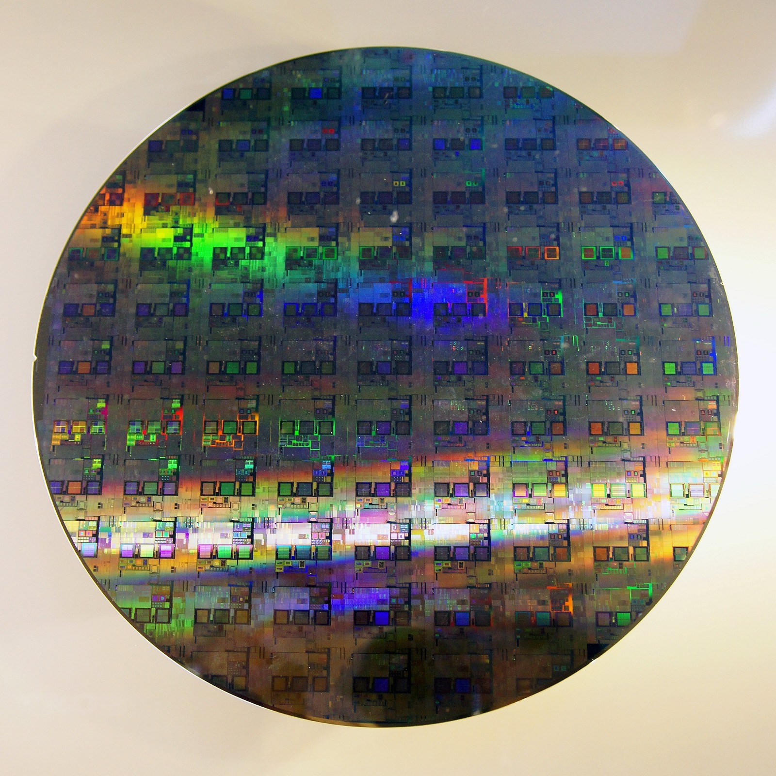 A 300mm silicon wafer. Before becoming HBM, dies like these are ground down to about 50 micrometers — thinner than a sheet of paper. Photo: Peellden, CC BY-SA 3.0, via Wikimedia Commons.
At 50 micrometers, silicon stops behaving like a rigid crystal and starts behaving like wet tissue paper — curling and warping under its own internal stress. The thinning process, called backgrinding, is utterly dominated by Japanese equipment makers, above all DISCO Corporation.
DISCO's machines perform a brutal yet delicate ballet. First a coarse grind with heavy diamond wheels strips away 80–90 percent of the bulk silicon; then a fine "poligrind" with superfine abrasives polishes the surface to a roughness measured in nanometers. Even so, grinding leaves microscopic stress marks that weaken the chip. To keep the wisp-thin silicon from shattering, manufacturers use tricks like DISCO's TAIKO process, which — instead of thinning the whole wafer evenly — leaves a 3-millimeter rigid ring around the rim, like the uncut crust of a pizza, to hold everything together while the center is shaved down.
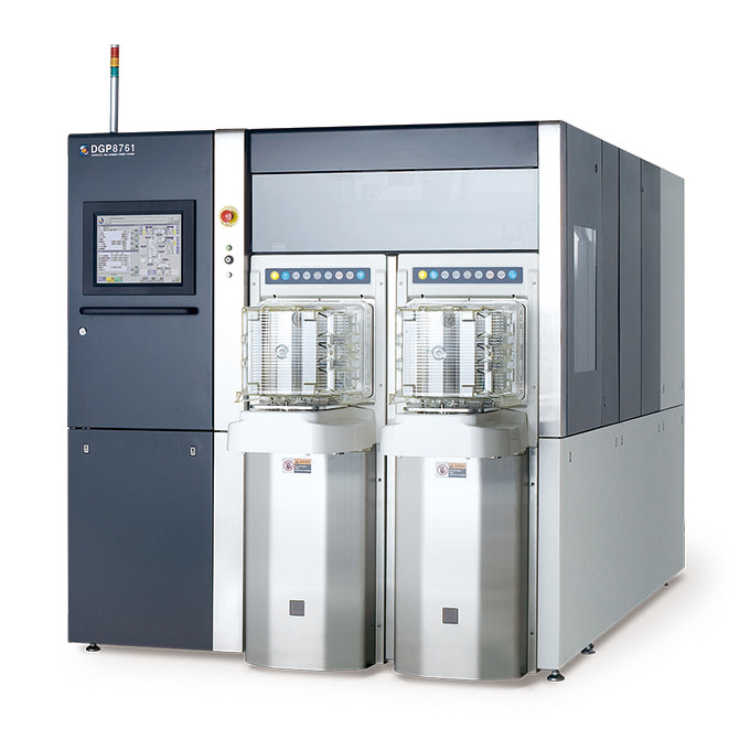 The machine behind the magic trick: a DISCO DGP8761 grinder/polisher, the kind of equipment that thins HBM wafers to a fraction of a hair's width. DISCO of Japan dominates this corner of the industry. Photo: DISCO Corporation.
The margin for error is essentially zero. Variation in thickness — what engineers track as Total Thickness Variation — has to be all but eliminated. A tiny vibration in the grinder, or a microscopic deformation in its spindle, can leave the silicon uneven by a few micrometers. That's enough to make the chips bond imperfectly when stacked, opening air voids that kill the chip.
The Japanese chemical monopoly
Once thinned, the silicon has to be drilled through with those through-silicon vias and polished perfectly flat. A single HBM3 die carries 1,024 active data TSVs, plus thousands more for power and grounding. Making each one means etching a microscopic hole clean through the silicon, insulating its walls, and electroplating it with copper — which has to fill the hole flawlessly from the bottom up. If just one TSV in a 16-layer stack fails to conduct, the entire vertical column goes dark.
Getting the surface flat enough requires Chemical Mechanical Planarization (CMP), a polishing process that depends on exquisitely specific "slurries" to level the wafer at the atomic scale. And here lies one of the most underappreciated chokepoints in all of technology: the world's supply of the ultra-pure ceria slurries needed for advanced CMP is dominated by a single Japanese company, Resonac (formerly Showa Denko). The photoresists that pattern the TSVs come mostly from Japan's Tokyo Ohka Kogyo and JSR. The blank 300mm silicon wafers themselves are cast largely by Japan's Shin-Etsu Chemical and SUMCO.
Follow the chain and the fragility is dizzying. The multi-trillion-dollar valuations of American AI giants rest on Nvidia GPUs, which rest on HBM from three memory vendors, which rest, in turn, on a handful of Japanese chemical vats.
The thermal interrogation
Because an HBM package bonds 12 to 16 expensive dies onto an even more expensive base logic die, catching a defective chip before it's stacked is a matter of economic life and death.
Stack one bad die and you've destroyed the whole package. "Consider the stacked die — one base logic, and then 8 to 16 HBM," explains an executive at Aehr Test Systems. "Making sure that base logic device is of the highest quality is critical, because if it's bad, 16 dies get thrown away. So it's a huge multiplier in the yield curve." So the industry has "shifted left" — moving its most rigorous testing out of the final assembly stage and onto the bare wafer, hunting for what it calls Known Good Dies, or KGD.
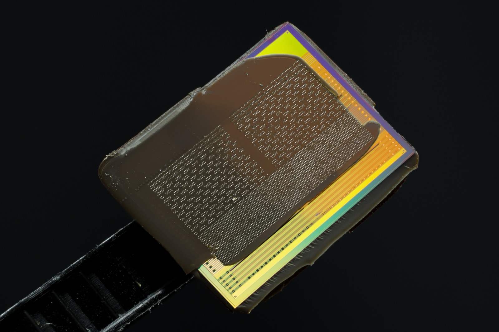 A decapped HBM DRAM die under the microscope. Each wafer-thin layer must prove flawless before it's allowed into a stack. Photo: Fritzchens Fritz, CC0 (public domain), via Wikimedia Commons.
This testing is brutally hard. As bandwidth climbs, the copper bumps connecting the dies — the "micro-bumps" — have to shrink. Today's HBM3E packs them at a pitch of 20 to 30 micrometers; HBM4 will squeeze that down toward 10. Traditional test probes — essentially tiny metal needles — are far too clumsy to land on arrays that dense without smashing the fragile pads.
Enter FormFactor, a California company that builds advanced MEMS (Micro-Electro-Mechanical Systems) probe cards. Instead of needles, its cards use microscopic, photolithographically printed vertical springs. During a test, the card touches down on thousands of microscopic pads at once, each spring applying a precisely calibrated 1 to 2.5 grams of force. Too much and you crush the pad; too little and the electrical connection fails.
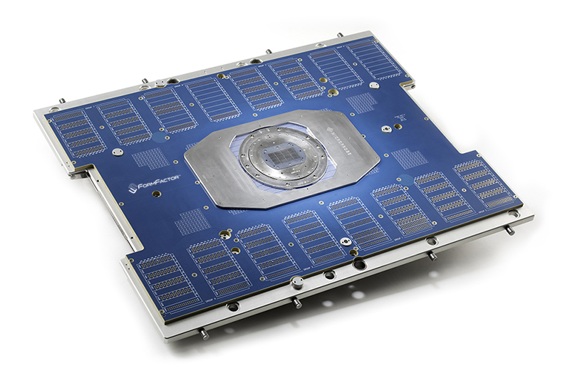 A FormFactor Apollo probe card. The silver head at the center holds thousands of microscopic, photolithographically made vertical springs that land on a chip's pads all at once — each pressing with just 1 to 2.5 grams of force. Photo: FormFactor, Inc. (used for editorial illustration).
There's a subtler menace, too: latent defects, the chip-world equivalent of "infant mortality." A die can pass a room-temperature test perfectly and then die a week later inside a 90°C AI server rack. To flush out these weaklings, manufacturers use Wafer-Level Burn-In (WLBI) — essentially torturing the silicon to find which units would have failed early.
Aehr Test Systems dominates this niche, and its approach is gleefully aggressive. Its FOX-XP system loads up to 18 full 300mm wafers into a chamber at once, bakes them at extreme temperatures, and pumps hundreds of amps of current through those microscopic MEMS probes — compressing months or years of operational stress into a few hours to expose any weak spot. Only dies that survive this interrogation earn the KGD badge and are cleared for stacking. Then automated test gear from the entrenched duopoly of Advantest and Teradyne runs the final electrical measurements.
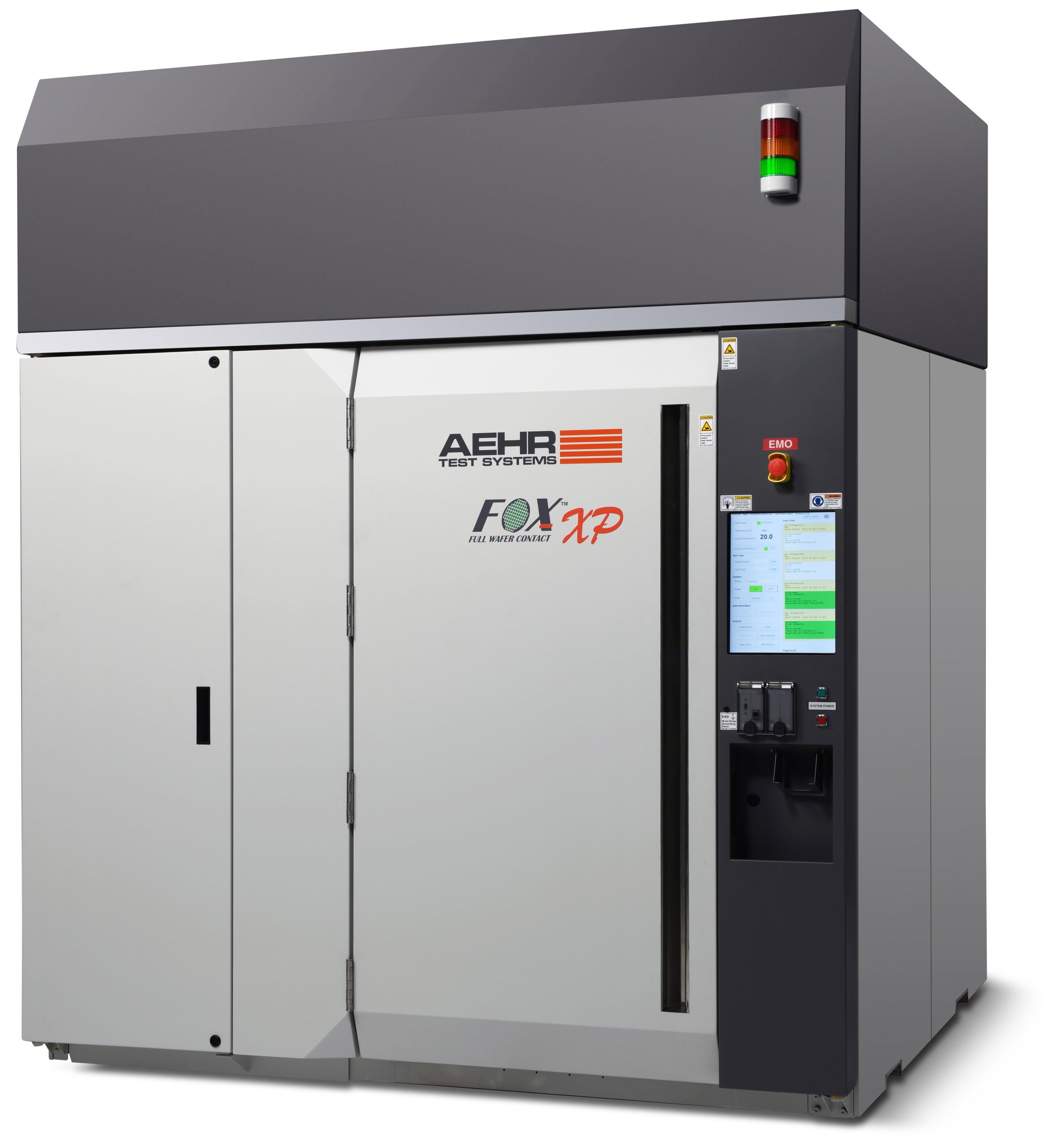 An Aehr Test Systems FOX-XP burn-in system. It can load up to 18 full wafers at once and bake them under extreme heat and current to flush out chips that would have failed early. Photo: Aehr Test Systems.
The bonding war: MR-MUF vs. TC-NCF
The single most fraught step in making HBM is the bonding — the actual gluing-together of the stack. At 1.15 terabytes per second, these dies run hot, and stacking them vertically traps that heat, especially in the middle layers. Let the temperature climb too high and the memory cells start leaking their electrical charge faster than they can be refreshed — and the AI accelerator stalls or crashes.
How a manufacturer bonds its chips, then, determines whether they survive. And it's exactly here that the fortunes of Samsung and SK Hynix split apart — rearranging the entire semiconductor pecking order.
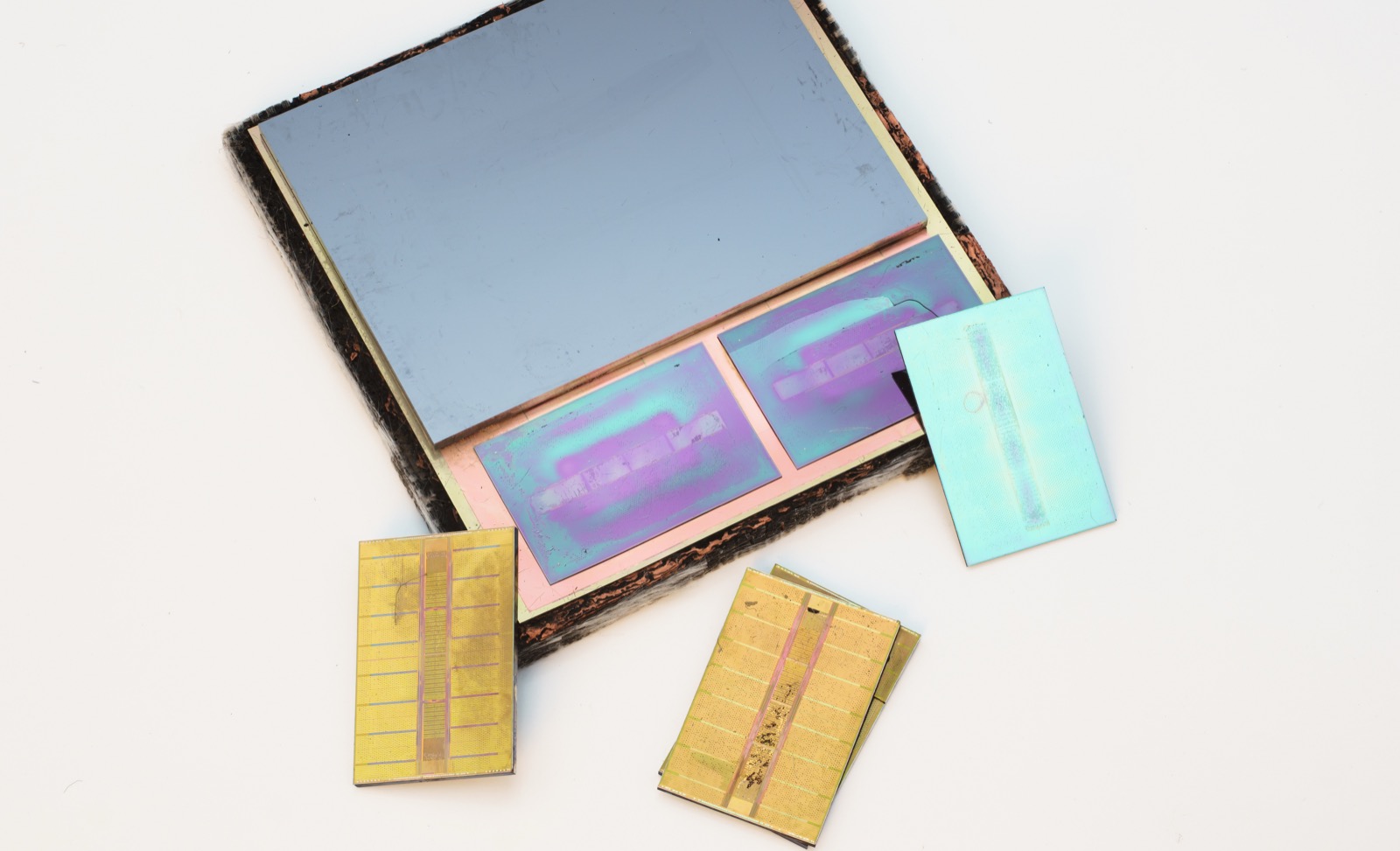 A GPU interposer with the HBM stacks removed, revealing the dense fields of micro-pads where memory and processor connect. How those connections are bonded is the industry's most contentious engineering question. Photo: Fritzchens Fritz, CC0 (public domain), via Wikimedia Commons.
Samsung and Micron rely on a well-established method called Thermal Compression with Non-Conductive Film (TC-NCF). A solid, non-conductive film is laid between each thinned die, then the dies are pressed together under high heat and immense pressure to melt the film and fuse the copper micro-bumps.
It worked — until stacks grew to 12 layers for HBM3E. The pressure needed to bond a dozen ultra-thin dies kept warping and cracking that 50-micrometer silicon. Worse, the non-conductive film acted as a thermal blanket, trapping heat inside the stack. That heat trap was the chief reason Samsung's 12-high HBM3E flunked Nvidia's strict heat-and-power qualification for nearly 18 months — a delay that cost Samsung the entire early procurement cycle for Nvidia's Blackwell chips and left it watching from the sidelines while SK Hynix ran away with the market.
SK Hynix had taken a riskier road years earlier, pioneering a process called Mass Reflow Molded Underfill (MR-MUF). Rather than pressing films between each layer one at a time, SK Hynix tacks all the dies in place with quick bursts of heat, then bakes the whole tower in a reflow oven to melt every solder bump at once — and finally injects a proprietary liquid epoxy into all the microscopic gaps in a single shot.
That epoxy — supplied exclusively by Japan's NAMICS Corporation — conducts heat about twice as well as the old non-conductive film. By skipping the high-pressure squeeze, SK Hynix eliminated die warpage entirely; the liquid flows cleanly around every bump, improving heat dissipation by 36 percent over earlier generations. MR-MUF is the technical reason SK Hynix sits on the HBM throne.
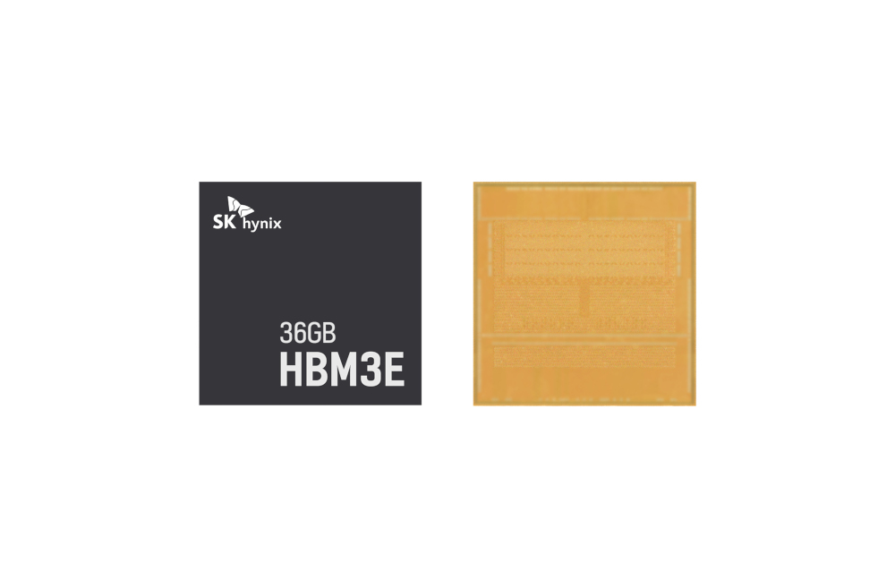 The prize at the center of it all: SK Hynix's 36GB, 12-layer HBM3E. The dark square is the finished package; beside it, the exposed stack of a dozen wafer-thin dies. Photo: SK hynix Inc.
But that dominance comes shackled to bespoke equipment. SK Hynix's bonders come from South Korea's Hanmi Semiconductor, which holds nearly 70 percent of that equipment market — and the relationship reveals just how cutthroat this business is. When SK Hynix recently tried to diversify by placing a $30 million bonder order with a challenger, Hanwha Semitech, Hanmi retaliated hard: it abruptly pulled its 50-to-60 service engineers off SK Hynix's production lines, hiked prices on existing gear by 25 percent, and sued Hanwha for patent infringement. In an industry where a single machine's calibration can swing yields by double digits — and billions in Nvidia orders hang on those yields — that's a knife fight.
The next frontier: HBM4 and the logic-die war
As the industry gears up to mass-produce the sixth generation, HBM4, in 2026 and 2027, the rulebook is being rewritten by two innovations: the smart base die, and hybrid bonding.
The rise of the custom base die
In HBM3 and HBM3E, that logic "base die" at the bottom of the stack was basically a dumb traffic cop, shuttling power and signals between the DRAM and the GPU. In HBM4, it's getting a brain. The base die will start absorbing memory controllers and compute functions that used to live on the GPU itself.
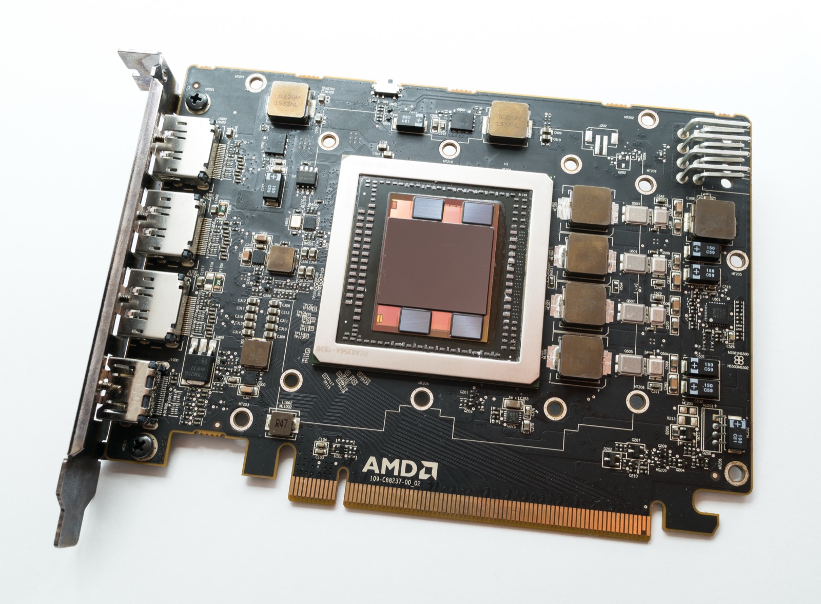 HBM stacks sit cheek-by-jowl with the GPU on this AMD Radeon R9 Nano package — the close physical pairing that defines the technology. In HBM4, the base die underneath each stack stops being a passive traffic cop and becomes an active compute layer. Photo: Fritzchens Fritz, CC0 (public domain), via Wikimedia Commons.
Because that base die now needs complex, high-speed logic, it can no longer be made on older, trailing-edge memory processes. It needs a leading-edge foundry — and that has touched off a proxy war between TSMC and Samsung Foundry.
SK Hynix has thrown in with TSMC, building its standard HBM4 logic dies on TSMC's 12nm node, and reportedly eyeing TSMC's cutting-edge 3nm process for the premium "Custom HBM4E" aimed at Nvidia's future Vera Rubin architecture.
Samsung — uniquely, the only player that makes both memory and logic chips in-house — is fighting back by keeping everything internal. It's putting standard HBM4 on its 4nm process and pushing hard to use its bleeding-edge 2nm GAA (Gate-All-Around) process for custom HBM4E dies. If it works, Samsung's 2nm base die could offer dramatically better power efficiency and thermal behavior than SK Hynix's TSMC-built silicon — potentially letting Samsung leapfrog its rival and reclaim the crown. It would also hand Samsung's struggling foundry guaranteed internal volume to improve yields at new fabs like its plant in Taylor, Texas.
Erasing the micro-bump: the hybrid-bonding revolution
There's a hard ceiling on how tall an HBM package can be. Standard HBM4 calls for stacking 16 memory dies — and even at 50-micrometer thinness, doing that with physical copper micro-bumps and underfill blows past the 775-micrometer JEDEC limit. (JEDEC is reportedly weighing a bump to 900 micrometers for temporary relief, but the micro-bumps themselves are failing: below a 10-micrometer pitch, the copper plating becomes wildly inconsistent.)
The endgame is hybrid bonding. Championed by equipment makers like the Netherlands' BESI and Austria's EV Group, it does away with solder micro-bumps entirely. Instead, the silicon surfaces are polished to atomic-level smoothness, pressed together at room temperature — where van der Waals forces bond the silicon oxide — and then gently annealed so the embedded copper pads expand and fuse directly into one another.
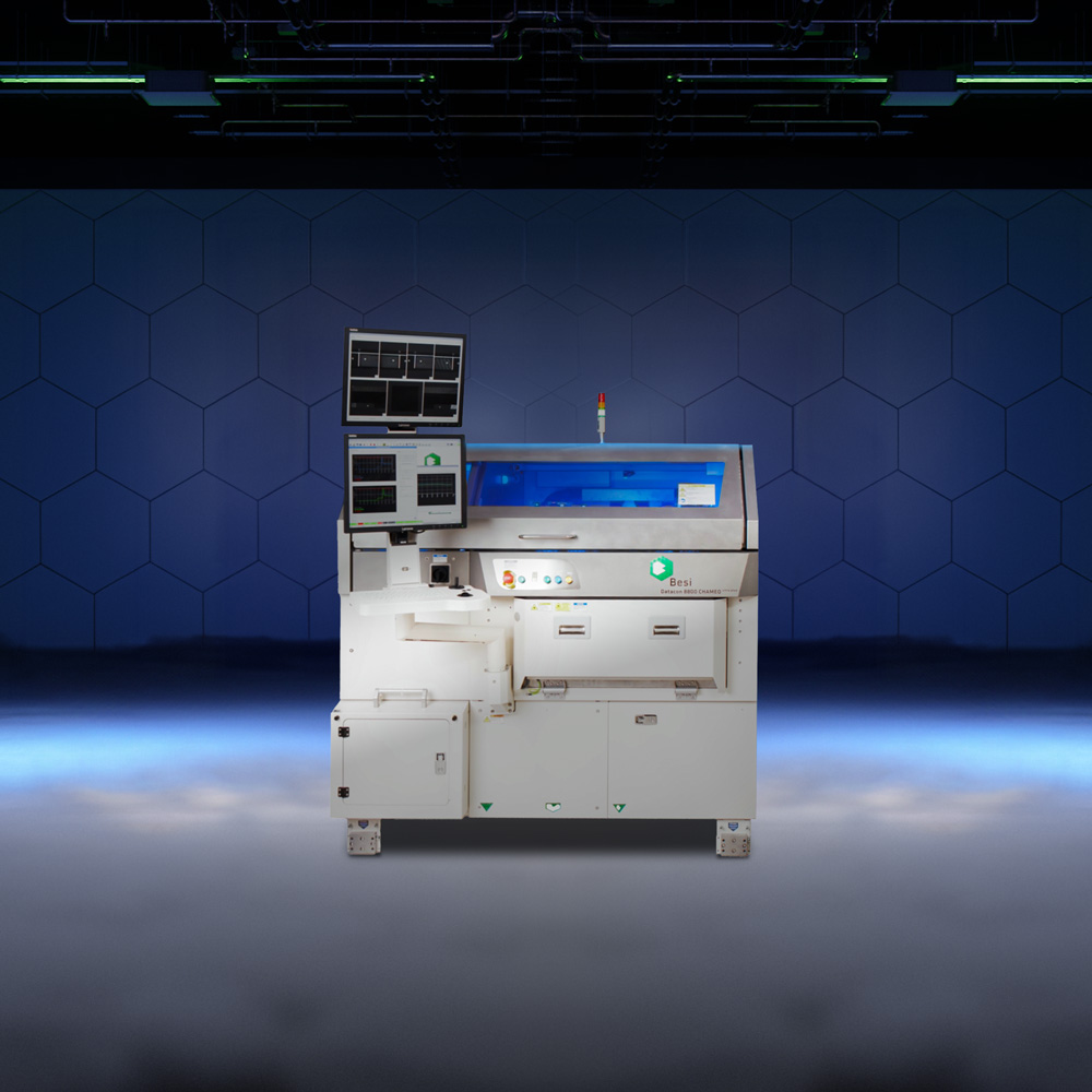 The tool that may rewrite HBM manufacturing: a BESI Datacon 8800 CHAMEO hybrid bonder, which fuses chips copper-to-copper with no solder bumps at all — but demands a near-perfect, dust-free cleanroom. Photo: BE Semiconductor Industries (Besi).
The result is a bump-less, copper-to-copper weld with zero gap between dies. It cuts thermal resistance by up to 47 percent, triples vertical heat conduction, and shaves more than 15 percent off the stack height, while allowing nearly unlimited interconnect density. The catch: it demands an almost impossibly pristine cleanroom. A single speck of dust on the bonding surface ruins the entire 16-layer stack.
Samsung is betting heavily on hybrid bonding as a Hail Mary to escape its TC-NCF heat problems. SK Hynix, meanwhile, is stubbornly squeezing MR-MUF for everything it's worth — recently placing a 44.2 billion won (~$32 million) order for next-gen Hanmi bonders, betting it can avoid the expensive, low-yield leap to hybrid bonding all the way through HBM4 and even HBM5. New entrants smell opportunity, too: South Korea's LG Electronics is reportedly building its own hybrid bonders, hoping to grab share from BESI as the technology goes mainstream around 2028.
The sovereign chokepoint: China's CXMT
While the US, Korea, and Taiwan own the leading edge, a giant is quietly closing the gap. Under severe US export controls designed to kneecap China's AI ambitions, Beijing has poured billions into building a domestic chip industry from scratch.
China's strategy stacks three homegrown layers: Huawei's Ascend 910C accelerators (made by SMIC on a constrained, DUV-based 7nm process), domestic software, and — crucially — high-bandwidth memory from ChangXin Memory Technologies, or CXMT.
Western analysts long assumed HBM's packaging complexity and dependence on Japanese chemicals would be a permanent firewall against China. They were wrong. By early 2026, CXMT had reached surprising parity on HBM3 and begun shipping working samples to Huawei. Its yields remain a state secret — almost certainly well below Korean levels — but when the state is footing the bill in the name of national security, commercial yield matters far less than availability.
To fund the scale-up, CXMT filed for a massive 29.5 billion yuan (~$4.1 billion) IPO on the Shanghai Stock Exchange, earmarked specifically for HBM. Running new facilities in Hefei, Beijing, and Shanghai, it's aiming for 300,000 12-inch wafers a month by the end of 2026 — roughly 20 to 25 percent of a Samsung or SK Hynix. If CXMT can scale HBM3 and eventually HBM3E, it removes the last and most critical bottleneck throttling Huawei's chips — narrowing the global AI-infrastructure gap to perhaps three years and largely neutralizing the intent of Washington's export controls. The likely result: a fully bifurcated, self-sufficient Chinese AI ecosystem.
The investor's dilemma: riding the "memflation" supercycle
For investors, HBM is a tantalizing — and treacherous — opportunity.
By early 2026, Wall Street had woken up. Exchange-traded funds focused on the space, above all the Roundhill Memory ETF (ticker: DRAM), saw astonishing inflows, blowing past $10 billion in assets in record time and tripling in value within months.
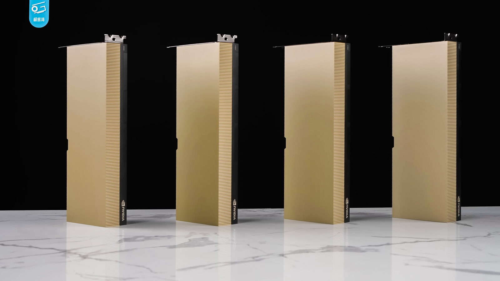 The product Wall Street is betting on: NVIDIA H100 accelerator cards. Each one carries stacks of HBM under its shroud, and the market for that memory is projected to grow more than tenfold in a single year. Photo: 极客湾Geekerwan, CC BY 3.0, via Wikimedia Commons.
The numbers justify some of the euphoria. The global HBM market, worth just $2.95 billion in 2025, is projected to hit somewhere between $24 billion and $54.6 billion in 2026, and as much as $70–100 billion by the 2030s — a compound annual growth rate north of 25 percent. Research firm Gartner expects total global semiconductor revenue to top $1.3 trillion in 2026, explicitly naming "memflation" — DRAM up 125 percent, NAND flash up 234 percent — as the main engine.
But sky-high valuations warrant caution. Micron's stock surged roughly 165 percent in early 2026 alone, stretching its price-to-sales ratio into nosebleed territory. Memory has always been a savage boom-and-bust commodity. The Roundhill DRAM ETF is extraordinarily concentrated — Samsung, SK Hynix, and Micron make up about 73 percent of it — and because the two Korean firms dominate, the fund doubles as a bet on the Korean won: a 5 percent swing in the won against the dollar can move the fund's value 2.5 percent before a single chip changes hands.
If hyperscaler capital-spending guidance (Amazon, Google, Meta, Microsoft) flattens, or a downturn slows enterprise AI, the resulting glut could send memory stocks down 40 to 60 percent in a matter of months — as they have in every prior cyclical bust.
And yet the bulls insist this time is different. The mass migration of factory capacity away from standard DDR5 and NAND toward HBM has created a genuine, physical shortage across all memory types. Because HBM is sold on multi-year contracts rather than the volatile spot market, suppliers have unprecedented revenue visibility — both SK Hynix and Micron say their entire 2026 HBM output was sold out and locked into non-cancellable pricing by mid-2025.
For patient investors, there's also a "pick-and-shovel" angle that sidesteps the memory cartel entirely: the equipment makers who hold monopolies on mission-critical steps. BESI (hybrid bonding), FormFactor (MEMS probe cards), Aehr Test Systems (wafer-level burn-in), and Teradyne (automated test) all profit no matter which memory maker wins. BESI alone is up 41 percent year-over-year, buoyed by rumors that American giants like Applied Materials are circling it.
The silicon ceiling
When Apple raised the price of the MacBook Neo and the iPad Air in the summer of 2026, it wasn't just protecting margins. It was passing the physical tax of the AI era down to the everyday consumer. The voracious appetite of hyperscale data centers has fundamentally broken the old consumer-electronics supply chain.
High Bandwidth Memory is no longer just a component. It has become the physical speed limit of technological progress itself. The choreography it demands — grinding silicon to the edge of transparency, drilling microscopic copper tunnels, testing under hundreds of amps with zero margin for error, binding it all with custom polymers — represents the absolute bleeding edge of what humanity can manufacture.
The companies that master this art — whether SK Hynix defending its thermal throne, Samsung attempting a 2nm leapfrog, or China's CXMT clawing toward sovereignty — will decide exactly how smart, and how fast, tomorrow's AI can become. For now, raw computing power is abundant. The memory to feed it remains frustratingly, and profitably, scarce.
Sources & further reading
- AP News — "Apple increases prices for Macs and iPads, blaming a shortage of memory chips." apnews.com
- The Guardian — "Apple raises iPad and MacBook prices, blaming cost of chips amid AI boom." theguardian.com
- CBS News — "Apple and Microsoft are raising their prices by hundreds of dollars as chip costs soar." cbsnews.com
- Al Jazeera — "Apple, Microsoft hike prices over surging chip costs." aljazeera.com
- EE Times — "How AI and Geopolitics Forge a Memory Market Crisis." eetimes.com
- EE Times — "How SK Hynix Redefined the Memory Market." eetimes.com
- EE Times — "MR-MUF Innovations Tackle Heat Generation." eetimes.com
- Semiconductor Engineering — "HBM Shifts Testing Left To Preserve AI Chip Yield." semiengineering.com
- Semiconductor Engineering — "HBM4 Sticks With Microbumps, Postponing Hybrid Bonding." semiengineering.com
- Semiconductor Engineering — "Making Hybrid Bonding Better." semiengineering.com
- TrendForce — "The HBM4 Battle Begins! Hybrid Bonding as the Key Breakthrough." trendforce.com
- TrendForce — "SK hynix Reportedly Places 44.2bn Won TC Bonder Order with Hanmi." trendforce.com
- TrendForce — "Samsung Reportedly Moves Custom HBM Logic Die to 2nm Foundry Process." trendforce.com
- Counterpoint Research — "Global DRAM and HBM Market Share: Quarterly." counterpointresearch.com
- Tom's Hardware — "SK hynix passes Samsung as South Korea's most valuable company." tomshardware.com
- Gartner — "Worldwide Semiconductor Revenue to Exceed $1.3 Trillion in 2026." gartner.com
- Wccftech — "China Closes HBM Gap With Korea To Just Three Years As CXMT Hits Technology Parity On HBM3." wccftech.com
- DISCO Corporation — "Governing Factors of Processing Quality for the Silicon Wafer Thinning Process." disco.co.jp
- DESCANSO / SemiconductorX, Aehr Test Systems, FormFactor, SK hynix Newsroom — corporate releases on HBM packaging, testing, and capacity.
Image credits
- AMD Fiji GPU package (hero) — C. Spille / pcgameshardware.de, CC BY-SA 4.0, via Wikimedia Commons.
- HBM cutaway schematic — ScotXW, CC BY-SA 4.0, via Wikimedia Commons.
- 300mm silicon wafer — Peellden, CC BY-SA 3.0, via Wikimedia Commons.
- HBM DRAM die close-up, GPU interposer, AMD Radeon R9 Nano package — Fritzchens Fritz, CC0 / public domain, via Wikimedia Commons.
- NVIDIA H100 accelerator — 极客湾 Geekerwan, CC BY 3.0, via Wikimedia Commons.
- DISCO DGP8761 grinder/polisher — DISCO Corporation (© DISCO; product image used for editorial illustration).
- FormFactor Apollo probe card — FormFactor, Inc. (© FormFactor; product image used for editorial illustration).
- Aehr FOX-XP burn-in system — Aehr Test Systems (© Aehr; product image used for editorial illustration).
- SK Hynix 36GB 12-layer HBM3E — SK hynix Inc. (© SK hynix; press/product image used for editorial illustration).
- BESI Datacon 8800 CHAMEO hybrid bonder — BE Semiconductor Industries (Besi) (© Besi; product image used for editorial illustration).