Building With Starlight: Inside the Impossible Physics of EUV Lithography
· 20 min read
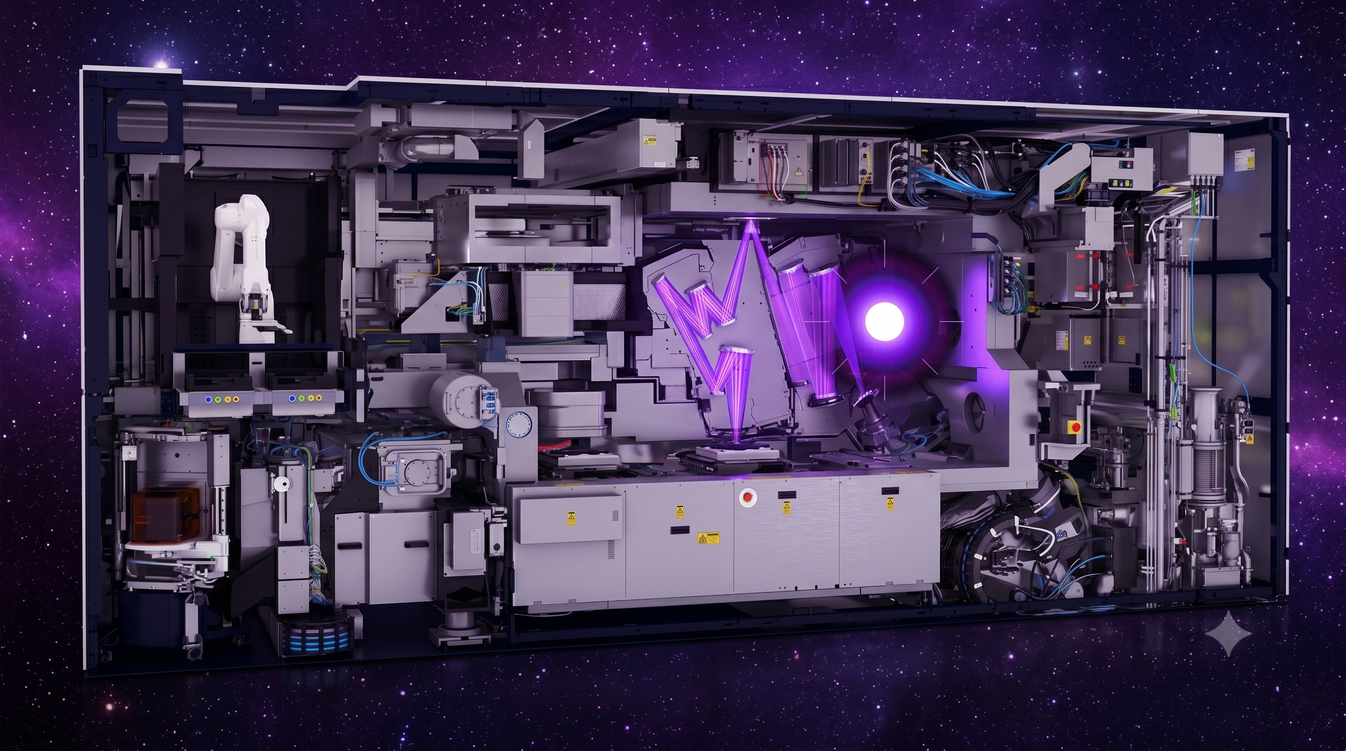
Somewhere inside a refrigerator-cold vacuum chamber in a windowless fab, a droplet of molten tin no bigger than a speck of dust is falling sideways at 150 miles per hour. A laser finds it, taps it once to flatten it into a tiny pancake, then hits it again with a pulse so violent the metal explodes into a plasma hotter than the surface of the sun. For a few billionths of a second, that microscopic fireball glows with a specific, rare color of light — and that flash is used to print a transistor.
Then it happens again. And again. Fifty thousand times a second, all day, for months on end.
This is Extreme Ultraviolet lithography — EUV — and the machines that do it are, by most reasonable measures, the most complex objects humans have ever mass-produced. A single one weighs as much as two fully loaded semi-trucks, contains hundreds of thousands of parts sourced from a planet-spanning supply chain, and carries a price tag that now tops $400 million. Exactly one company on Earth — the Dutch firm ASML, a spin-off of Philips — knows how to build them. Without these machines, there is no iPhone, no AI boom, no modern GPU. With them, Moore's Law gets to live another decade.
Here's how the impossible gets done, one component at a time.
01 — The Wall: Why 193-Nanometer Light Ran Out of Road
For half a century, chipmaking has run on a simple trick: photolithography, essentially a microscopic printing press. You shine light through a stencil (the "mask") of a circuit pattern, shrink that pattern with lenses, and project it onto a silicon wafer coated in light-sensitive chemicals. Wherever the light lands, the chemistry changes, and you etch the design into the chip. To make smaller transistors, you use a sharper "pen" — that is, a shorter wavelength of light.
For years that pen was a 193-nanometer beam from an argon-fluoride excimer laser, a workhorse called deep ultraviolet, or DUV. Engineers squeezed extraordinary performance out of it with tricks like immersion (projecting the light through a thin layer of water to bend it more sharply) and multi-patterning (exposing the same wafer several times to weave finer features together). But below roughly the 10-nanometer mark, physics slammed the door. A 193-nm wave is simply too fat a brush to paint atomic-scale detail. You can't draw a hair with a paint roller.
The escape route was to switch on a far shorter pen: light at 13.5 nanometers. That's more than fourteen times shorter than DUV — an enormous leap across the electromagnetic spectrum. It is also where the trouble starts, because light that energetic is absorbed by almost everything it touches, including glass lenses, including the air in the room. To use it, the industry had to reinvent every single step of the printing process from scratch.
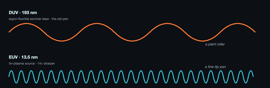
Fig. 1 · The Wavelength Leap. One wave, fourteen times tighter. The same horizontal span holds far more EUV crests than DUV — and more crests means finer detail. Switching pens is the whole ballgame, but 13.5-nm light is so energetic it's swallowed by glass and air alike, forcing a top-to-bottom redesign of the machine.
02 — The Light Source: How to Bottle a Star, 50,000 Times a Second
The first problem is brutal: there is no laser that simply emits powerful, sustained 13.5-nm light. So engineers make it the hard way, by building a tiny artificial star. The method is a Laser-Produced Plasma source, and it works exactly as outlandishly as it sounds — drop molten tin into a vacuum and obliterate it with a laser until it flashes with extreme ultraviolet.
Why tin, and why 13.5 nm
Tin was chosen after years of materials hunting because of a quirk of its atoms. Strip a tin atom of eight to thirteen of its electrons — into highly charged states physicists label Sn⁹⁺ through Sn¹⁴⁺ — and as the remaining electrons cascade between specific inner-shell energy levels, they spit out photons. The math of those particular transitions clusters the emitted light into a sharp spike right around 13.5 nanometers, clean enough to print with. Tin, essentially, is tuned to the exact color the machine needs.
The droplet generator
Inside the source vessel, a generator fires a continuous stream of molten-tin spheres, each far smaller than the width of a human hair, sailing across the chamber at over 240 kilometers per hour — and it does this 50,000 times every second. Hitting a target that small, that fast, that often is a targeting problem of almost comic difficulty. An array of cameras, sensors and tracking lasers — the "vessel metrology" — watches every droplet and nudges the aim tens of thousands of times a second to keep the shots landing.
The master laser
The gun is the largest industrial laser ever built, made by Germany's TRUMPF in partnership with ASML. It weighs more than 10 metric tons, contains over 450,000 parts, and pushes a carbon-dioxide beam past 10 kilowatts of average power. It starts from a seed pulse of just a few watts and runs it through five massive amplifier stages, multiplying the power more than 10,000-fold until peak pulses spike into the multi-megawatt range.
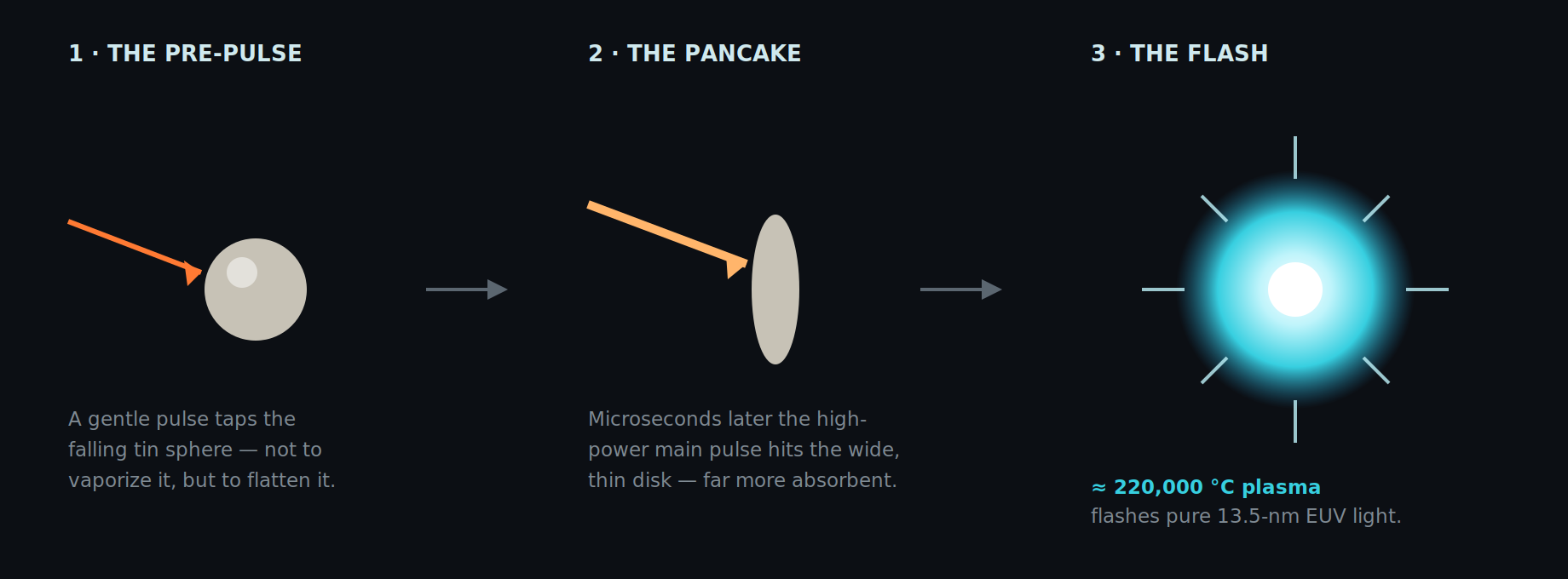
Fig. 2 · The Double-Shot. Two shots, not one. A single hard hit would just scatter the tin. So the laser fires a choreographed pair — a soft pre-pulse to flatten the droplet into a disk, then a main pulse the flattened target absorbs efficiently — ripping it into a plasma 30 to 40 times hotter than the sun's surface. Miss the timing by a fraction of a microsecond and the plasma never ignites.
"If the light arrives a fraction of a microsecond too early or too late, the second shot misses entirely. The whole machine lives or dies on that timing."
By the numbers
- 50,000 — Tin droplets vaporized per second
- 220,000°C — Plasma temperature — 30–40× the sun's surface
- 10 tons — Weight of the TRUMPF master laser
- 450,000+ — Parts in the laser alone
03 — Debris & The Collector: Catching the Light Without Wrecking the Mirror
Once the plasma flares, it throws EUV light in every direction at once. A huge curved mirror called the collector has to scoop up that scattered glow and funnel it toward the rest of the machine. The geometry is elegant: the plasma sits at one focal point of an ellipse, and the mirror reflects everything into a tight beam at a second focal point — the "intermediate focus," where the light officially enters the scanner. The same coating also filters out unwanted infrared from the CO₂ laser.
But that fireball is filthy. Blasting tin at 220,000 °C sprays high-speed ions, vapor, microscopic particles and even splashes of molten metal straight at the collector. And the collector is absurdly sensitive: a tin film just one nanometer thick — a few atoms — cuts its reflectivity by 20 percent. In the earliest prototype machines, an unprotected collector was ruined in 60 seconds. To run a fab, ASML needed collectors that survive for months.
A self-cleaning chemistry trick
The fix is part airbag, part chemistry set. The chamber is flooded with low-pressure hydrogen gas (around 100 pascals). Mechanically, the gas acts like a microscopic cushion, slowing the incoming tin ions and sweeping the debris toward "tin catcher" exhaust pumps. Chemically, the intense EUV light splits hydrogen molecules into highly reactive hydrogen radicals. When those radicals meet stray tin atoms sitting on the mirror, they react to form stannane — a gas — which simply floats off the surface and gets vacuumed away.
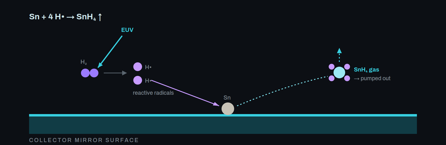
Fig. 3 · The Self-Cleaning Mirror. Tin in, gas out. EUV light cracks hydrogen into radicals that chemically lift deposited tin off the mirror as stannane gas — a continuous self-clean that stretches collector life from under a minute to many months. The catch: those same tiny hydrogen atoms burrow into the mirror's coatings and can blister them, which is why researchers are eyeing inert helium as an alternative.
04 — The Optics: Mirrors Polished to the Size of an Atom
Because 13.5-nm light is eaten by glass, the centuries-old refractive lens is useless here. EUV machines see by reflection only — and the whole light path, source to wafer, sits in a hard vacuum so the air can't absorb the beam. Every mirror is built by ASML's optics partner, Germany's ZEISS, and each one is a small miracle.
The Bragg trick
A household mirror is a single metal layer. At 13.5 nm that would reflect roughly 1 percent of the light — bounce off a few of those and your beam is gone. So ZEISS builds distributed Bragg reflectors: up to 100 alternating layers of molybdenum and silicon, each only a few atoms thick. A sliver of light reflects at every boundary, and because the layer spacing is precisely tuned to 13.5 nm, all those tiny reflections come back out in phase and reinforce each other. The result is about 70 percent reflectivity per mirror — enough to survive the journey.
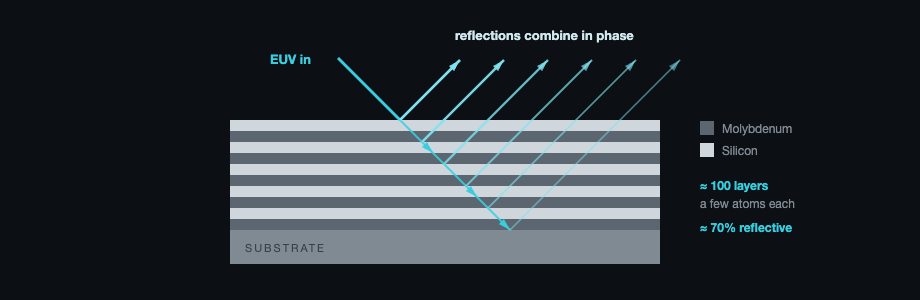
Fig. 4 · The Bragg Multilayer Mirror. A mirror made of math. No single surface can reflect EUV well, so ~100 atom-thin molybdenum/silicon layers each contribute a sliver of reflection that adds up — constructive interference, tuned to one wavelength. Any bump on the surface ruins the wavefront, so ZEISS polishes the substrates to literal atomic flatness.
Flatter than a continent
At this wavelength, the faintest bump distorts the image. So ZEISS polishes its mirror substrates to a smoothness that's hard to even picture. The standard comparison: scale one of these projection mirrors up to the size of Germany, and its tallest defect — the equivalent of the country's highest peak — would stand just one-tenth of a millimeter tall. Verifying that perfection takes 150-ton measuring machines inside 5-by-10-meter vacuum chambers, and several months per mirror.
Then the mirrors have to hold still. Six big mirrors ride inside the projection optics on a mechatronic system of some 20,000 parts, constantly adjusting for heat and the vibration of the wafer stage whipping around just below. The stability is unreal: if one of these mirrors sat on Earth and aimed a laser at the Moon, it could hold the spot steady on a target the size of a ping-pong ball.
"Scale the mirror up to the size of Germany, and its biggest flaw would be a tenth of a millimeter tall."
05 — The Mask & Pellicle: Guarding the Blueprint From a Single Speck of Dust
The circuit blueprint lives on a photomask. In DUV, light shines through the mask. In EUV, where everything reflects, the mask itself is a mirror — the same molybdenum/silicon Bragg stack, capped with a thin layer of ruthenium to fight corrosion, then topped with a tantalum-based absorber that defines the actual pattern. The light strikes it at a shallow 6-degree angle. A single blank costs around $300,000.
Now the nightmare: the same mask prints the same pattern onto chip after chip after chip. So one stray dust particle on the mask doesn't ruin one chip — it ruins every chip, a "repeater" defect that can wipe out an entire wafer of expensive processors. In DUV this is solved cheaply with a pellicle, a transparent film suspended a few millimeters above the mask; dust lands on the film, far out of focus, and never prints.
The pellicle from hell
EUV makes that trivial film nearly impossible. Ordinary transparent plastics absorb 13.5-nm light greedily, and because the mask reflects, the beam must pass through the pellicle twice. That double-pass dumps so much energy that the membrane heats to between 600 and 1,000 °C in a vacuum, where there's no air to carry the heat away. Early polysilicon films thin enough to stay transparent (under 50 nm) were so fragile they tended to rupture.
The breakthrough came from Belgium's nanoelectronics hub Imec and Japan's Mitsui Chemicals: a pellicle woven from carbon nanotubes. Rolled-up sheets of graphene, CNTs are stronger than steel at a fraction of the weight and shrug off 1,000 °C without sagging. They transmit better than 95 percent of EUV light, survive next-gen sources pushing past a kilowatt, and — unlike polysilicon — are transparent enough that standard inspection tools can see right through them. Mitsui has stood up mass production, and even TSMC is repurposing old fabs to make its own.
Table 1 · Pellicle Showdown
| Property | Polysilicon (early) | Carbon Nanotube (now) |
|---|---|---|
| Material | Silicon film, ~50 nm | Woven graphene cylinders |
| Strength | Highly fragile | ~100× stronger than steel |
| EUV transmittance | ~90.6% | ≥ 94% (up to 97.7%) |
| Inspection light (DUV) | Opaque — must retract | Transparent — see-through |
| Power tolerance | ~400 W | 600 W to 1 kW |
06 — The Wafer Stage: Moving the Canvas on a Cushion of Magnetism
While the optics project the pattern down, the silicon wafer below has to move to catch it — not in a smooth sweep but a rapid, stop-and-go "step-and-scan," exposing one rectangular field, jumping to the next, and repeating until the whole 300-mm disk is covered. ASML's "Twinscan" design runs two stages: while one wafer is being exposed, a second is in a metrology bay being mapped in 3D, because no wafer is perfectly flat. When the stages swap, the optics already know every microscopic hill and valley to keep focus razor-sharp.
Friction is the enemy. Old DUV stages floated on air bearings, like an air-hockey table — but EUV's vacuum makes air bearings impossible. Instead the stage levitates on magnetism, hovering over a floating permanent-magnet plate that can weigh 1,400 kilograms, driven by electromagnetic coils so it glides frictionlessly through the vacuum.
The tracking is the staggering part. Sensors bounce light off a precision grid to read the stage's position in all six degrees of freedom, correcting it 20,000 times a second and holding alignment to within a quarter of a nanometer. It has to: an overlay error of a few nanometers between chip layers means short circuits and dead silicon. ASML's recent machines hold matched overlay near 1.1 nanometers — and the newest High-NA tools have pushed that to 0.7.
07 — The Quantum Catch: When You Can Count the Photons, Randomness Bites Back
Perfect light, perfectly aimed at a perfectly placed wafer, is still useless if the chemical film recording the image can't keep up. That film is the photoresist, and at EUV scales it runs into a problem rooted in quantum mechanics itself.
Recall the Planck–Einstein relation, E = hc / λ: a photon's energy rises as its wavelength shrinks. Each 13.5-nm EUV photon therefore carries about 14 times the punch of a DUV photon (roughly 92 electron-volts versus 6.4). The total dose you can deliver is fixed by how fast the scanner runs — so because each photon is so energetic, it takes far fewer of them to expose the resist. And when you're counting individual photons, randomness starts to show.
This is photon shot noise. A flood of weak DUV photons wets the resist evenly, like a steady downpour soaking a sidewalk. EUV is more like a sparse scatter of heavy raindrops — by pure chance, some spots get a few extra hits and some get none. At single-nanometer scales, those statistical gaps become real defects: jagged line edges, two wires accidentally bridging into a short, or a contact hole that never opens at all.
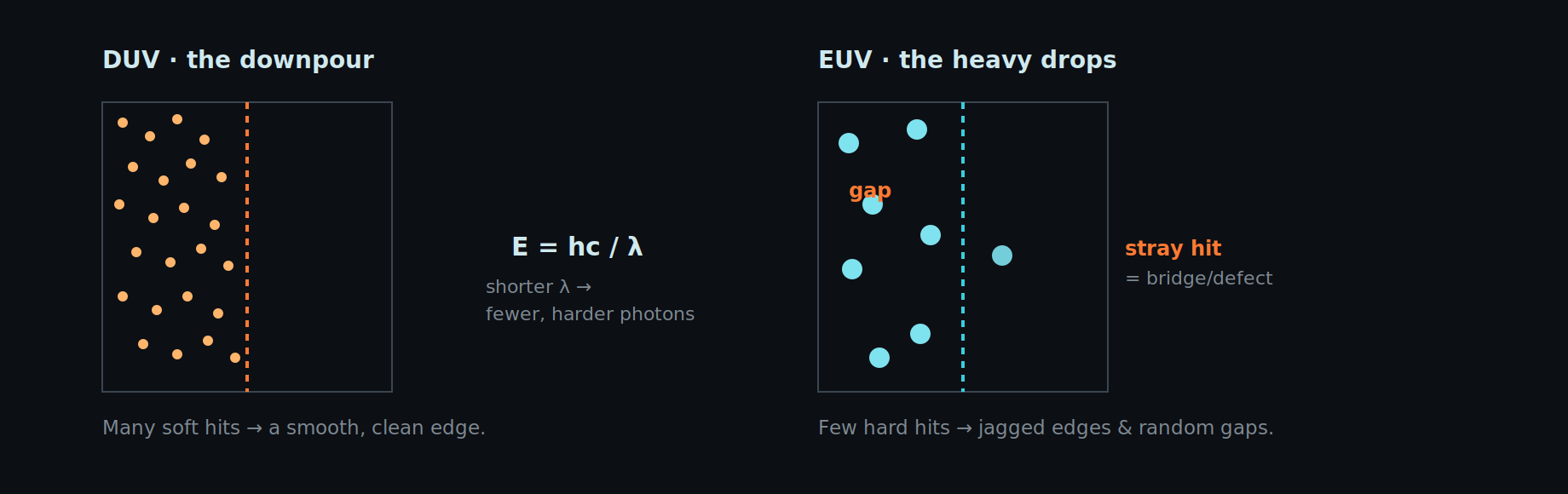
Fig. 5 · Photon Shot Noise. Statistics, not optics. These are random, non-repeating failures that happen even when the image is in perfect focus. The cure can't just be "more light" — that slows the scanner and kills the economics. The answer is a smarter resist.
The dry-resist revolution
Traditional resists are organic liquids spun onto the wafer, full of bulky polymer chains scattered at random — which compounds the randomness. The new approach, pioneered by Lam Research and JSR with platforms like Aether, ditches the liquid entirely. Metal-organic dry resist is laid down as a vapor by chemical vapor deposition, condensing into an ultra-thin, uniform film. Packing it with heavy, EUV-hungry atoms like tin or hafnium makes it absorb far more of those sparse photons, directly fighting shot noise, while the uniform deposition sharpens line edges and skips several bake-and-develop steps along the way.
08 — The Next Wall: High-NA, Anamorphic Optics, and a Reticle at 32 G
Even today's standard EUV — ASML's NXE line, now pushing 160–170 wafers an hour — bottoms out near a 13-nm resolution at a numerical aperture of 0.33. To reach the 2-nanometer node and the "Angstrom era" beyond, chipmakers need roughly 8-nm resolution. Since the wavelength is locked at 13.5 nm, the only knob left is the numerical aperture. So ASML and ZEISS raised it from 0.33 to 0.55 — High-NA — using bigger mirrors to gather light from wider angles. And that nearly broke everything.
The 3D shadow problem
Wider light cones mean steeper angles hitting the mask. Keep the old 4× shrink factor, and the incidence angle climbs from 6 to 9 degrees — steep enough that the tall absorber pattern on the 3D mask casts shadows across the reflective layers below, blurring and shifting the very features you're trying to sharpen. A bigger mask could fix it, but that would mean scrapping decades of globally standardized, multi-billion-dollar mask infrastructure. A non-starter.
The anamorphic save
The fix is delightfully strange: shrink the image unevenly. High-NA optics demagnify 4× in one direction but 8× in the other — an "anamorphic" lens, the same idea old CinemaScope movies used to squeeze a widescreen image onto standard film. I'm sure some of you wanna-be cinematographers and videographers know about anamorphic lenses. That keeps the light angle at a safe 6 degrees, sidesteps the shadows, and lets the industry keep its standard 6-inch mask.
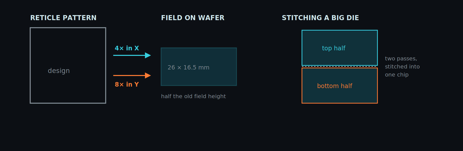
Fig. 6 · Anamorphic Optics & Field Stitching. Squeeze it sideways. The anamorphic 4×/8× shrink saves the mask but halves the exposure field — so the biggest chips (think giant AI accelerators) must be printed in two passes and stitched together with software-corrected, near-seamless borders.
And the reticle flies at 32 G
Halving the field means twice as many scans to cover a wafer, which would gut throughput. To claw it back, ASML cranked the stages: in the High-NA EXE machines, the wafer stage accelerates twice as hard as before — and the reticle stage hits an astonishing 32 G. For scale, that's like a Formula 1 car going 0–100 km/h in 0.09 seconds. Slinging a delicate reticle back and forth at 32 G, thousands of times an hour, in a vacuum, without shaking the sub-nanometer alignment loose, is about as hard as mechatronics gets. The whole 0.55-NA tool weighs 165 tons and needs a new cleanroom built around it.
Table 2 · Standard EUV vs. High-NA EUV
| Parameter | NXE:3600D (0.33 NA) | EXE:5000/5200 (0.55 NA) |
|---|---|---|
| Numerical aperture | 0.33 | 0.55 (High-NA) |
| Target resolution | ~13 nm | 8 nm |
| Magnification | 4× uniform | 4× / 8× anamorphic |
| Reticle acceleration | ~8 G (baseline) | 32 G |
| Throughput | ~160 wph | 175 wph → tunable past 200 |
| Matched overlay | 1.1 nm | 0.7 nm |
Dispatch · Where It Stands in 2026
High-NA goes live
High-NA EUV has crossed from the lab into the fab. In December 2025, Intel completed acceptance testing of the first commercial second-generation tool, the TWINSCAN EXE:5200B, at its D1X fab in Hillsboro, Oregon — the foundation for its 14A node, the first to lean on High-NA for its most critical layers, with risk production targeted for 2027. The machine is rated at 175 wafers per hour, which Intel plans to tune past 200, at a record 0.7-nm overlay.
It's no longer Intel's story alone. SK hynix became the first memory maker to install a commercial High-NA system in late 2025; Samsung took delivery of its first EXE:5200B around the same time for its 1.4-nm node; and Belgium's Imec secured a tool for sub-2-nm research, targeting qualification by the end of 2026.
ASML's roadmap doesn't stop there — successive EXE upgrades aim for 190-plus wafers an hour, and the company has floated an even more extreme "hyper-NA" 0.75 generation around 2032. Each of these tools costs roughly $400 million.
09 — The Takeaway: The Most Complicated Thing We Make
Step back and the whole machine reads like a dare against physics. A star ignited 50,000 times a second from flattened tin droplets. A fireball tamed by radical hydrogen chemistry. Mirrors flatter than a polished continent, held steadier than a laser aimed at the Moon. A pellicle woven from graphene that laughs off 1,000 degrees. A resist re-engineered to beat quantum randomness. And optics that squeeze an image sideways while flinging a mask at 32 G — all coordinated to print features a few atoms wide, layer over layer, with nanometer alignment, on a tool the weight of a fighter jet.
None of it comes from one company or one country. It's ASML at the center, but it runs on TRUMPF's lasers, ZEISS's optics, Imec and Mitsui's nanotubes, Lam and JSR's chemistry, and a hundred suppliers most people will never hear of. That a global web of specialists can make this work at all — let alone reliably enough to churn out the world's chips — is the quiet wonder behind every phone and data center.
As the features shrink toward the width of a few dozen atoms, the margin for error effectively vanishes. EUV lithography doesn't just draw the blueprint of the modern world. Right now, it defines the outer edge of what humans can physically build.
Selected Sources
- ASML — Lithography principles; EUV systems; "5 things about High-NA EUV"
- ZEISS SMT — EUV & High-NA EUV lithography
- TRUMPF — "EUV technology breakthrough thanks to master laser"
- Imec — "Sailing along the stochastic cliffs"; High-NA EUVL
- Intel Newsroom — High-NA EUV at Intel Foundry
- Wikipedia — Extreme ultraviolet lithography
- NIST SP 1500-208 — EUV Lithography Working Group report
- Semiconductor Engineering — "EUV Pellicles Finally Ready"
- STROBE / Univ. Colorado — Introduction to EUV Sources
- Mitsui Chemicals; SPIE; ASML SEC filings
- 2025–26 reporting: Tom's Hardware, TrendForce, TechPowerUp (EXE:5200B installs at Intel, SK hynix, Samsung, Imec)